- 您现在的位置:买卖IC网 > Sheet目录487 > NTD5802NT4G (ON Semiconductor)MOSFET N-CH 40V 16.4A DPAK
�� �
�
�NTD5802N,� NVD5802N�
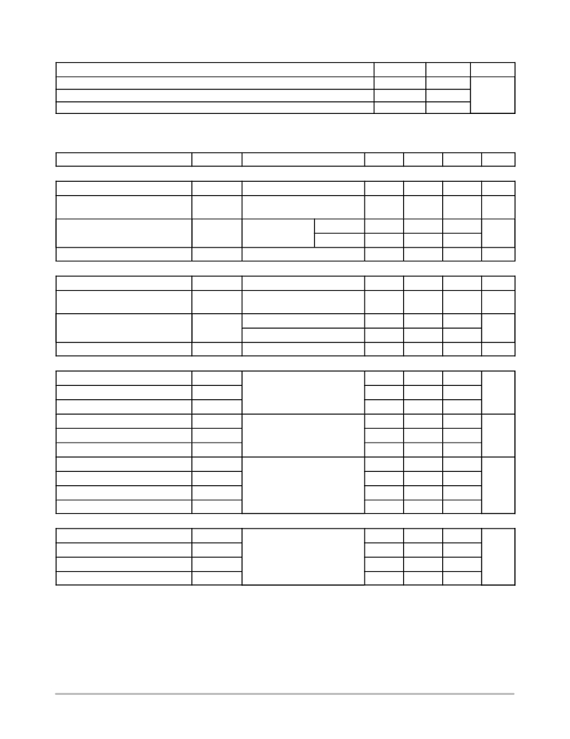
�THERMAL� RESISTANCE� MAXIMUM� RATINGS�
�Parameter�
�Junction� ?� to� ?� Case� (Drain)�
�Junction� ?� to� ?� Ambient� ?� Steady� State� (Note� 1)�
�Junction� ?� to� ?� Ambient� ?� Steady� State� (Note� 2)�
�Symbol�
�R� q� JC�
�R� q� JA�
�R� q� JA�
�Value�
�1.6�
�60�
�105�
�Unit�
�°� C/W�
�1.� Surface� ?� mounted� on� FR4� board� using� 1� in� sq� pad� size,� 1� oz� Cu.�
�2.� Surface� ?� mounted� on� FR4� board� using� the� minimum� recommended� pad� size.�
�ELECTRICAL� CHARACTERISTICS� (T� J� =� 25� °� C� unless� otherwise� noted)�
�Parameter�
�Symbol�
�Test� Condition�
�Min�
�Typ�
�Max�
�Unit�
�OFF� CHARACTERISTICS�
�Drain� ?� to� ?� Source� Breakdown� Voltage�
�Drain� ?� to� ?� Source� Breakdown� Voltage�
�Temperature� Coefficient�
�V� (BR)DSS�
�V� (BR)DSS� /T� J�
�V� GS� =� 0� V,� I� D� =� 10� m� A�
�40�
�40�
�V�
�mV/� °� C�
�Zero� Gate� Voltage� Drain� Current�
�I� DSS�
�V� GS� =� 0� V,�
�V� DS� =� 40� V�
�T� J� =� 25� °� C�
�T� J� =� 150� °� C�
�1.0�
�50�
�m� A�
�Gate� ?� to� ?� Source� Leakage� Current�
�I� GSS�
�V� DS� =� 0� V,� V� GS� =� "� 20� V�
�"� 100�
�nA�
�ON� CHARACTERISTICS� (Note� 3)�
�Gate� Threshold� Voltage�
�Negative� Threshold� Temperature�
�Coefficient�
�V� GS(TH)�
�V� GS(TH)� /T� J�
�V� GS� =� V� DS� ,� I� D� =� 250� m� A�
�1.5�
�?� 7.4�
�3.5�
�V�
�mV/� °� C�
�Drain� ?� to� ?� Source� On� Resistance�
�R� DS(on)�
�V� GS� =� 10� V,� I� D� =� 50� A�
�3.6�
�4.4�
�m� W�
�V� GS� =� 5.0� V,� I� D� =� 50� A�
�6.5�
�7.8�
�Forward� Transconductance�
�gFS�
�V� DS� =� 15� V,� I� D� =� 15� A�
�16.8�
�S�
�CHARGES� AND� CAPACITANCES�
�Input� Capacitance�
�C� iss�
�5300�
�pF�
�Output� Capacitance�
�Reverse� Transfer� Capacitance�
�C� oss�
�C� rss�
�V� GS� =� 0� V,� f� =� 1.0� MHz,�
�V� DS� =� 12� V�
�850�
�550�
�Input� Capacitance�
�Output� Capacitance�
�Reverse� Transfer� Capacitance�
�C� iss�
�C� oss�
�C� rss�
�V� GS� =� 0� V,� f� =� 1.0� MHz,�
�V� DS� =� 25� V�
�5025�
�580�
�400�
�pF�
�Total� Gate� Charge�
�Threshold� Gate� Charge�
�Gate� ?� to� ?� Source� Charge�
�Gate� ?� to� ?� Drain� Charge�
�Q� G(TOT)�
�Q� G(TH)�
�Q� GS�
�Q� GD�
�V� GS� =� 10� V,� V� DS� =� 15� V,�
�I� D� =� 50� A�
�75�
�6.0�
�18�
�15�
�100�
�nC�
�SWITCHING� CHARACTERISTICS� (Note� 4)�
�Turn� ?� On� Delay� Time�
�t� d(on)�
�14�
�ns�
�Rise� Time�
�Turn� ?� Off� Delay� Time�
�Fall� Time�
�t� r�
�t� d(off)�
�t� f�
�V� GS� =� 10� V,� V� DS� =� 20� V,�
�I� D� =� 50� A,� R� G� =� 2.0� W�
�52�
�39�
�8.5�
�3.� Pulse� Test:� Pulse� Width� ≤� 300� m� s,� Duty� Cycle� ≤� 2%.�
�4.� Switching� characteristics� are� independent� of� operating� junction� temperatures.�
�http://onsemi.com�
�2�
�发布紧急采购,3分钟左右您将得到回复。
相关PDF资料
NTD5803NT4G
MOSFET N-CH 40V 76A DPAK
NTD5804NT4G
MOSFET N-CH 40V 69A DPAK
NTD5805NT4G
MOSFET N-CH 40V 51A DPAK
NTD5806NT4G
MOSFET N-CH 40V 33A DPAK
NTD5807NT4G
MOSFET N-CH 40V 23A DPAK
NTD5862NT4G
MOSFET N-CH 60V 90A DPAK
NTD5865N-1G
MOSFET N-CH 60V 34A 18MOHM DPAK
NTD5865NL-1G
MOSFET N-CH 60V 40A 16MOHM IPAK
相关代理商/技术参数
NTD5803N
制造商:ONSEMI 制造商全称:ON Semiconductor 功能描述:Power MOSFET 40 V, 76 A, Single N−Channel, DPAK
NTD5803NG
制造商:ONSEMI 制造商全称:ON Semiconductor 功能描述:Power MOSFET 40 V, 76 A, Single N−Channel, DPAK
NTD5803NT4G
功能描述:MOSFET NFET DPAK 40V 75A 7.4mOhm RoHS:否 制造商:STMicroelectronics 晶体管极性:N-Channel 汲极/源极击穿电压:650 V 闸/源击穿电压:25 V 漏极连续电流:130 A 电阻汲极/源极 RDS(导通):0.014 Ohms 配置:Single 最大工作温度: 安装风格:Through Hole 封装 / 箱体:Max247 封装:Tube
NTD5804N
制造商:ONSEMI 制造商全称:ON Semiconductor 功能描述:Power MOSFET 40 V, 69 A, Single N−Channel, DPAK
NTD5804NG
制造商:ONSEMI 制造商全称:ON Semiconductor 功能描述:Power MOSFET 40 V, 69 A, Single N−Channel, DPAK
NTD5804NT4G
功能描述:MOSFET NFET DPAK 40V 69A 8.5mOhm RoHS:否 制造商:STMicroelectronics 晶体管极性:N-Channel 汲极/源极击穿电压:650 V 闸/源击穿电压:25 V 漏极连续电流:130 A 电阻汲极/源极 RDS(导通):0.014 Ohms 配置:Single 最大工作温度: 安装风格:Through Hole 封装 / 箱体:Max247 封装:Tube
NTD5805N
制造商:ONSEMI 制造商全称:ON Semiconductor 功能描述:Power MOSFET 40 V, 51 A, Single N−Channel, DPAK
NTD5805N_12
制造商:ONSEMI 制造商全称:ON Semiconductor 功能描述:Power MOSFET 40 V, 51 A, Single N.Channel, DPAK